For the longest time I used a $20 soldering iron that had the tip radius of a crayon. I assembled about 30 custom arduino nano boards with this iron. I have since downgraded to an iron that I found in the trash, but it came with several different tips, so it has led to an increase in the precision of my soldering. I will buy a good iron when I need to. That time has not yet come.
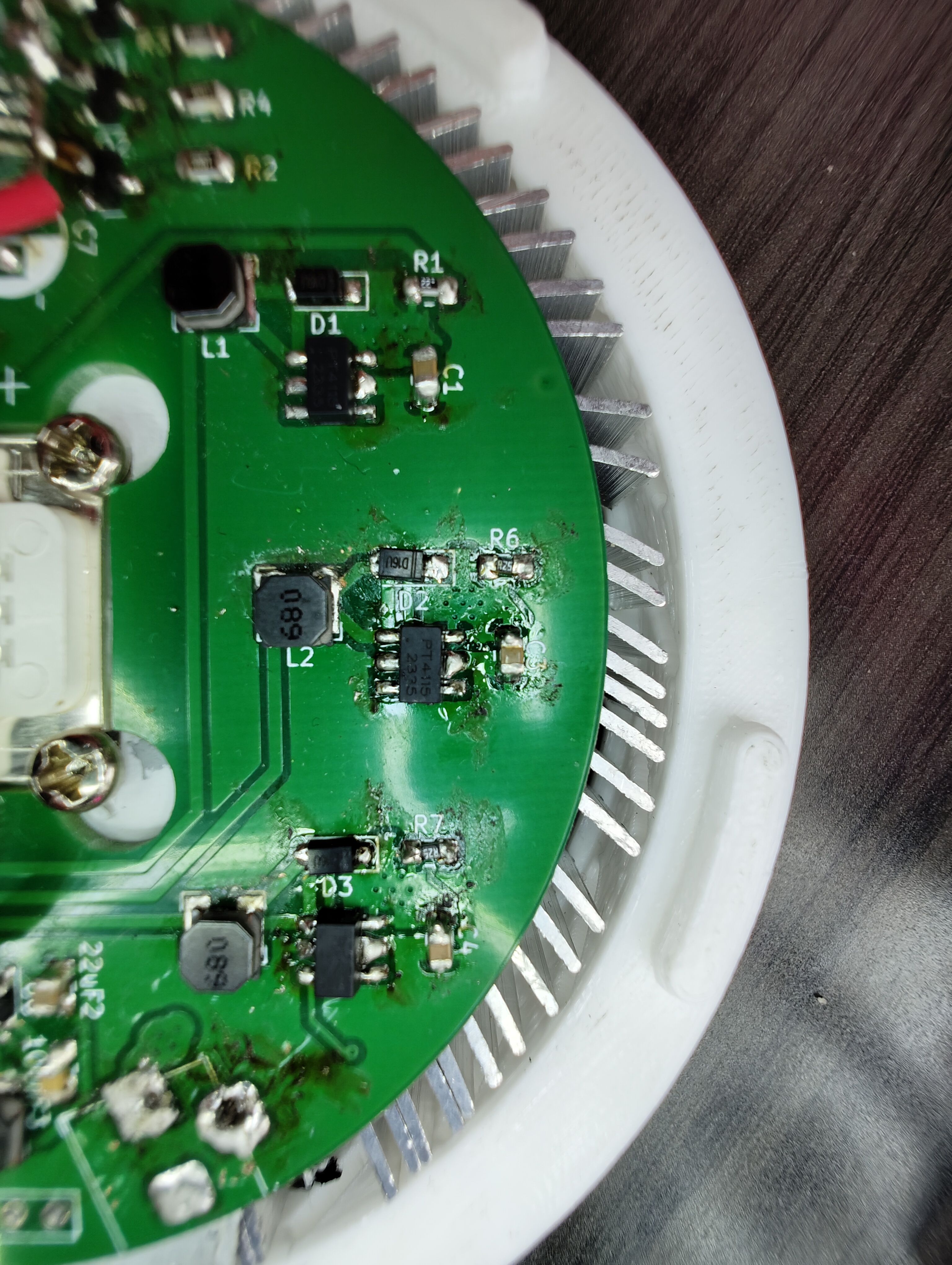
I have assembled 5 of these boards with all 53 components. The atmega chip is challenging because it has high pin density. The PT4115 driver is challenging because it has a large thermal relief pad that is difficult to get hot enough for a good bond. The inductors are difficult because their footprints are almost exactly the size of the package, leaving a small area for the iron to contact and heat it up. (Fully assembled PCB in next image below)
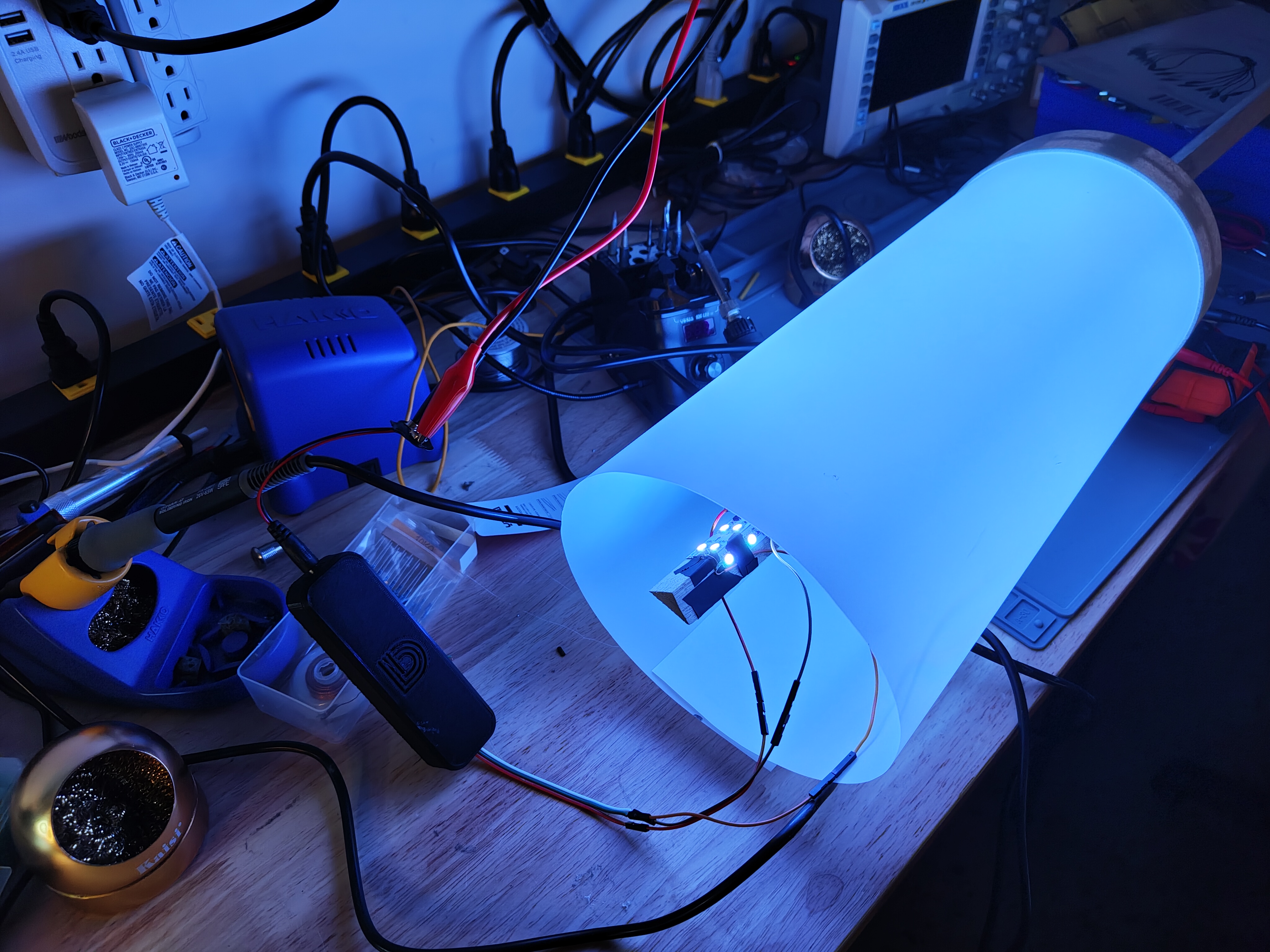
Learn more about this lamp and my lighting project here.
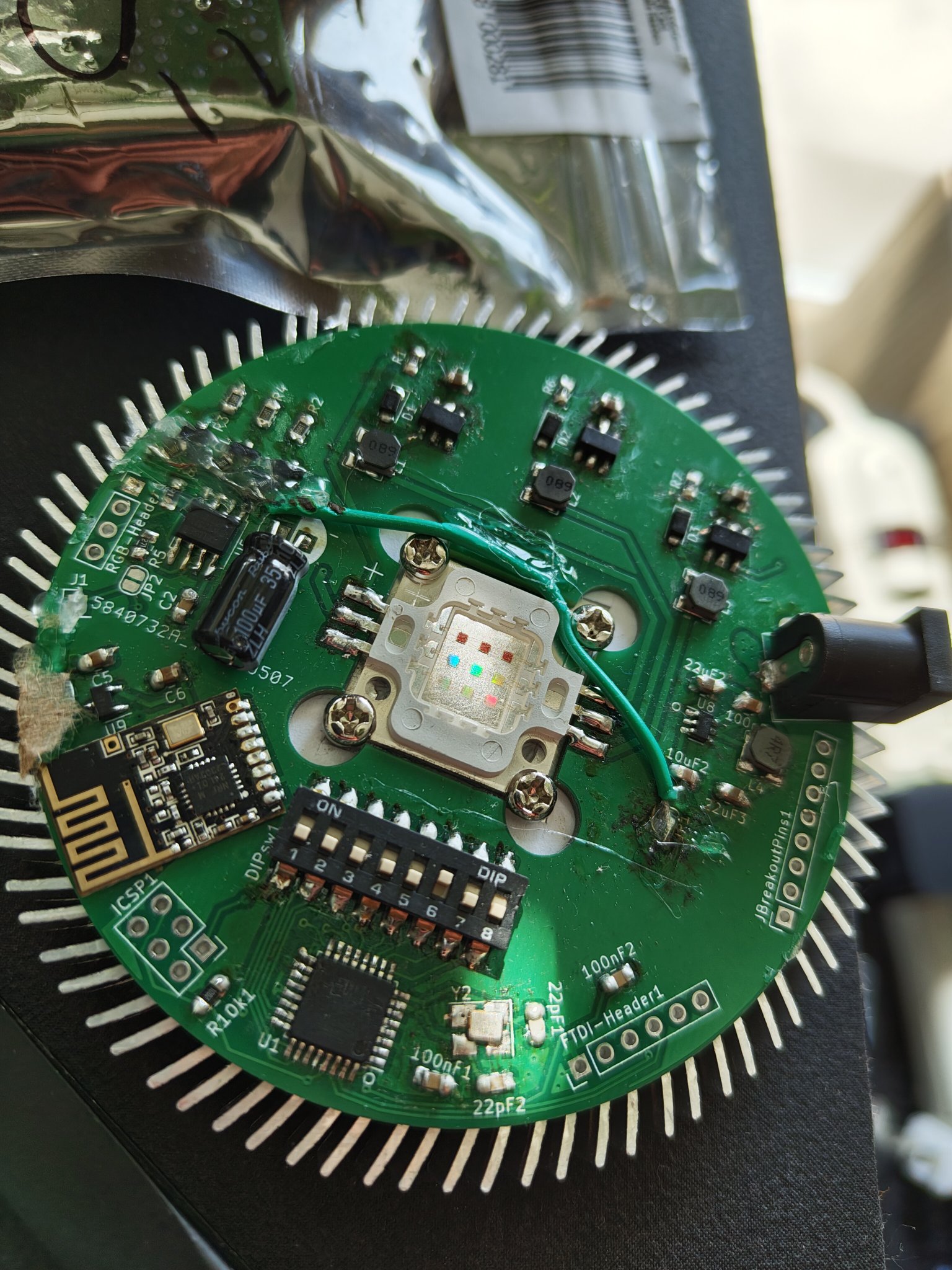
I was winging the first iteration of this board. I wanted to make a 10W RGB LED driver board and was copying designs online. Nobody was posting schematics as they were all selling their product that I was trying to make. I reverse engineered their schematics from the product listing pictures and implemented that on my own designs. The WS2811 LED driver that then triggers the high power LED drivers operates in an open sink mode. This chip is meant to operate on the low side of an LED and I didn't consider that in my initial design. I retroactively added pullup resistors to give the voltage differential that the PT4115 drivers required as their input signal since they were looking for more of a PWM type signal rather than a current sink signal.
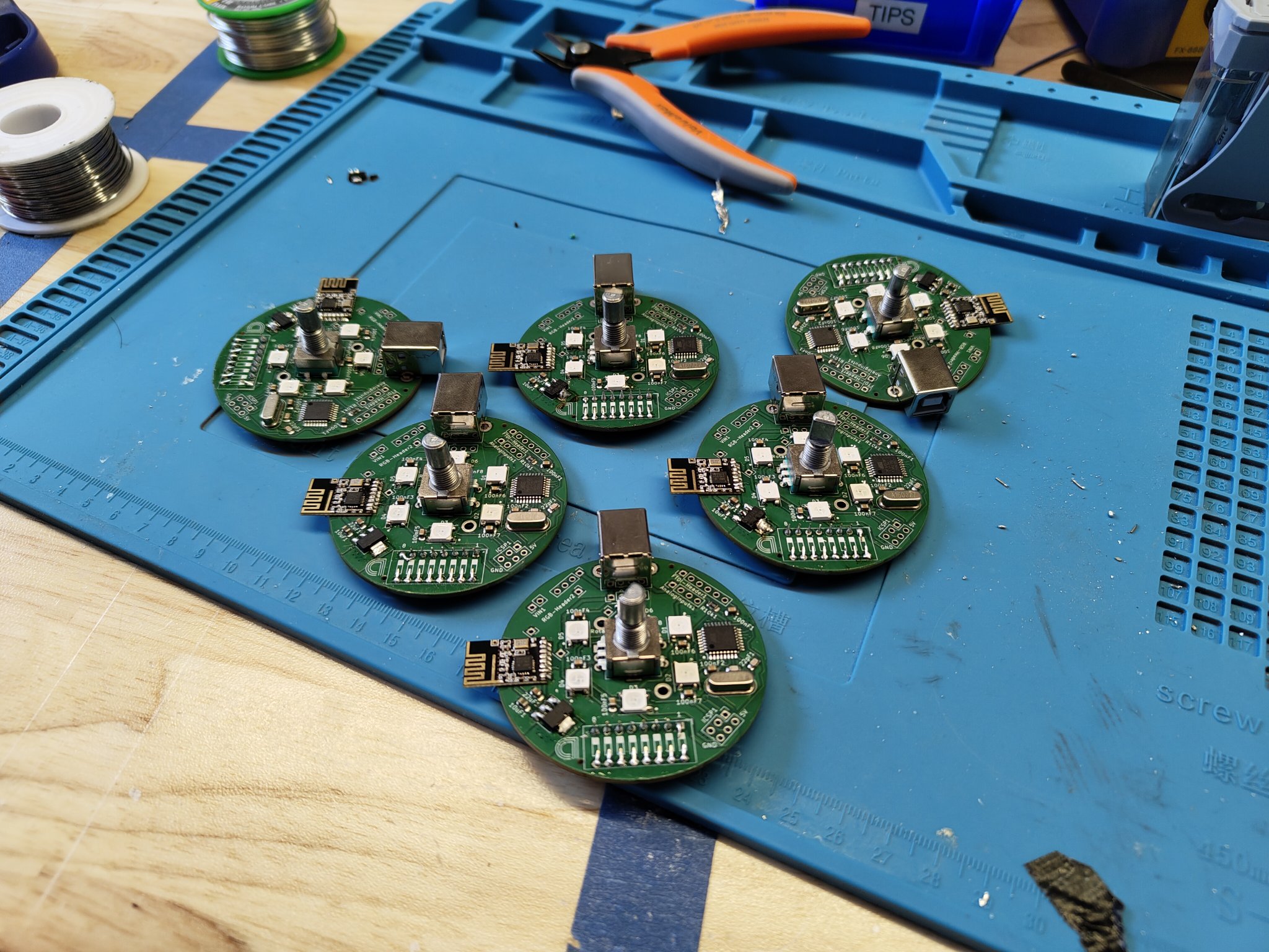
I have assembled 20 of these boards from a partially assembled state. (I learned my lesson and had the factory put on the decoupling caps and the atmega chip.) I had to add the LEDs on manually as well as the rotary encoder and usb port. I used dessicants and left the LEDs in a warm, dry place before attaching them to the board to avoid damage due to steam formation in the LED while soldering.
See this remote in action here.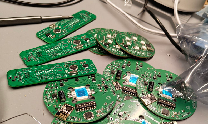
The stick pcbs are the ones on the left.
This was an early pcb design in my kicad learning process. I bought 50 blank boards and thought I would have a blast assembling all of them. In the 1.5 years I have had these boards, I've assembled about 30 (with the crayon iron). The most challenging part is attaching the atmega328p chip.
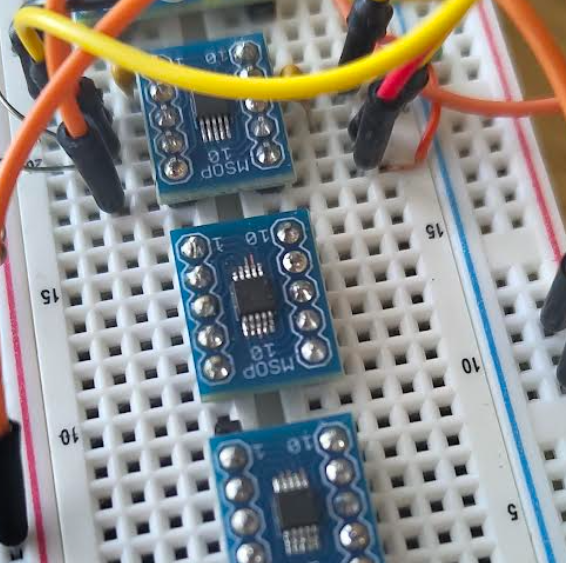
This is the smallest pin pitch that I have ever soldered on. The pins on this chip are 0.5mm apart. I bought breakout boards for them so I could breadboard my project design before sending it off to fab. I used my iron to apply small amounts of wire solder onto all 10 pads (I did not have solder paste or a mask at that time) then scraped the iron across their surface to ensure the pads were level. Finally, I used a heat gun while holding the chip onto the breakout board with pliers to heat the solder and attach the chip.
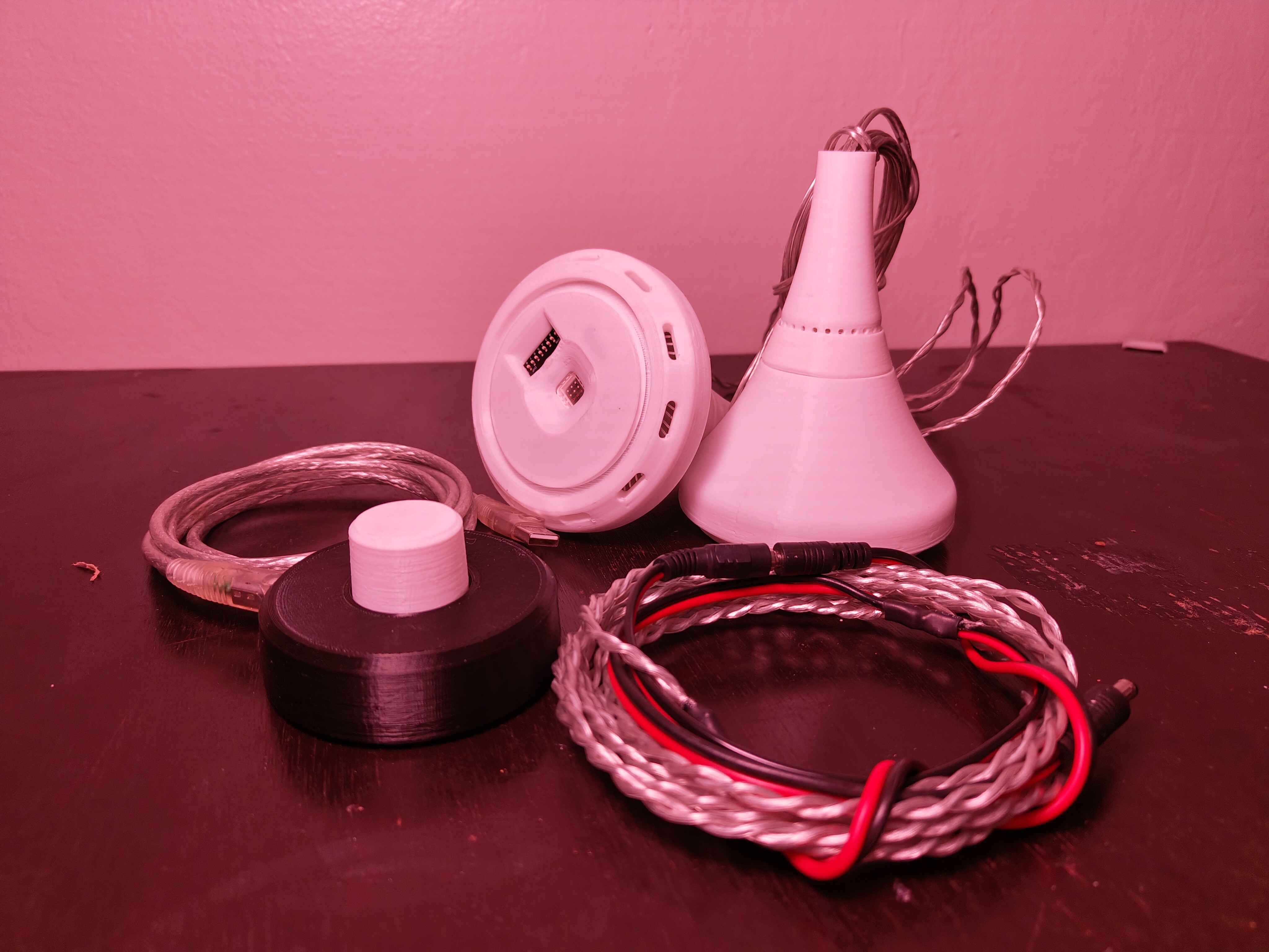
The cable is the silvery/clear bundle on the right. It has one input port and two output ports, the first next to the input, and the second at the end of the extension wire.
I make these splitter/extension cables to allow the user to connect multiple lamps to one power supply. I used 14-16awg wire throughout the cable assembly so up to 5 lamps can be connected with these cables. I typically use a heatgun to preheat the exposed parts of the wires, then move in with a soldering iron to actually apply the solder. I then finish the task by applying heat shrink and pump it full with hot glue to provide an even better mechanical connection.
This is a documentation of some of the places I have soldered.
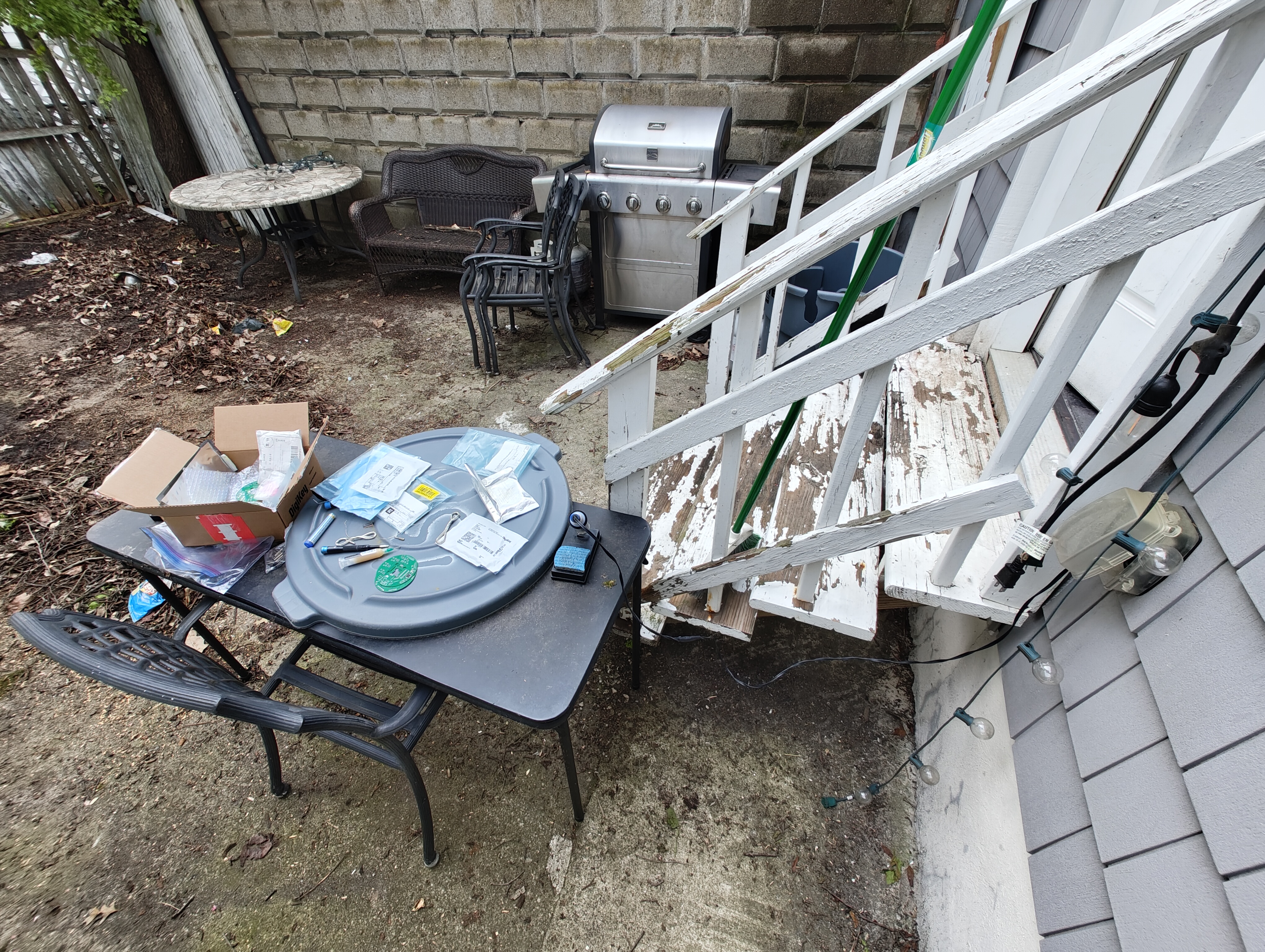
I was living in Boston for a few weeks and had to make do. The table surface was moldy so had to use trashcan lid to stabilize it.
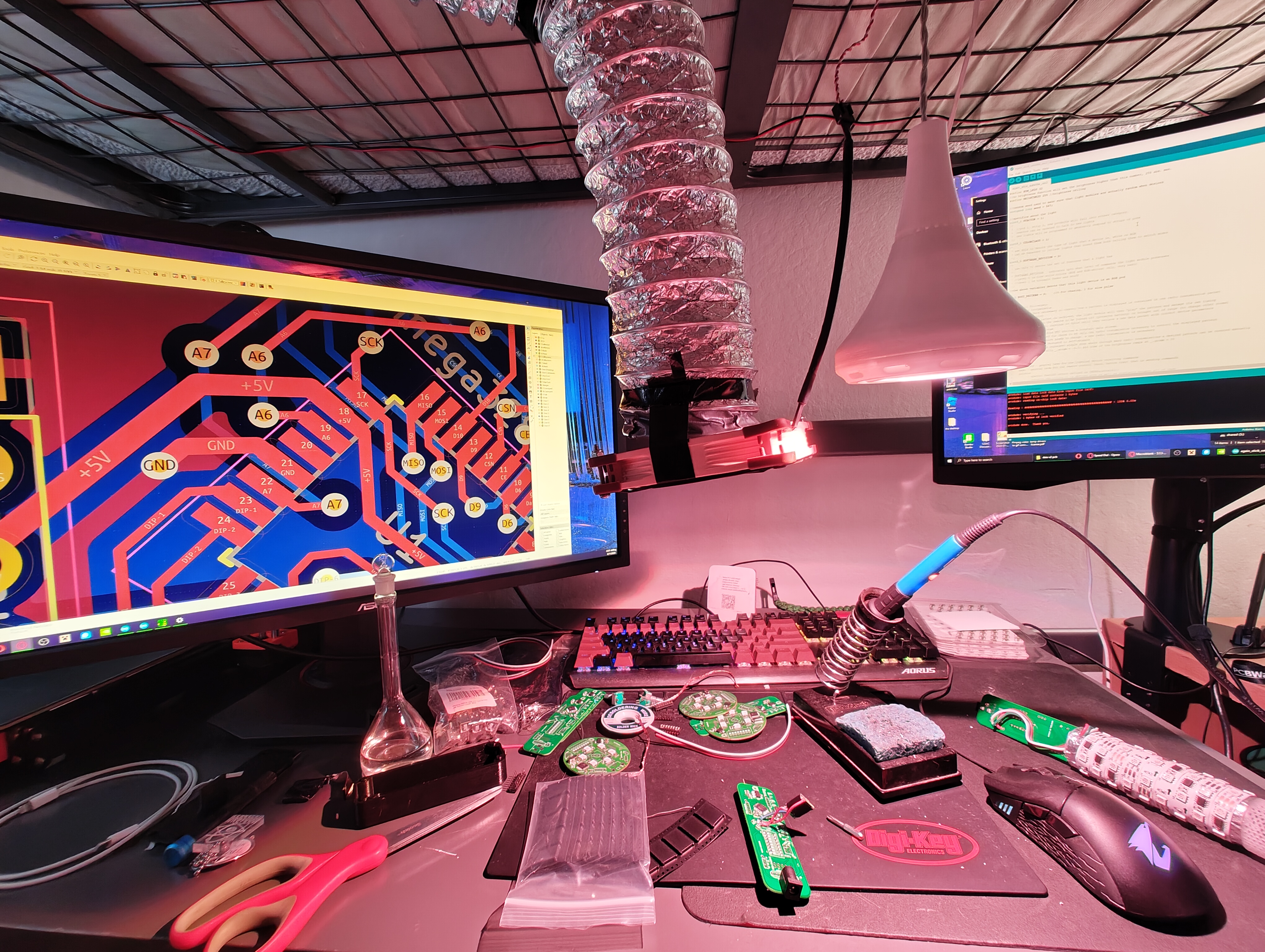
I found a loft bed on the side of the road and put my desk under it so I could hang stuff off the ceiling for extra utility.